Christian Doppler Laboratory for Direct Fabrication of 3D Nano-Probes – CDL DEFINE

More Information about Harald Plank
In March 2018, the Christian Doppler Laboratory for Direct-Write Fabrication of 3D Nano-Probes (CDL DEFINE) was officially opened under the auspices of Rector Univ.-Prof. DI Dr. Harald Kainz at Graz University of Technology. The origin of that CDL goes back to the long-lasting collaboration with the Austrian company GETec Microscopy GmbH (Vienna), whose product line is centered around highly compact Atomic Force Microscopes (AFM), specifically designed for the seamless integration in highly space-confined Scanning Electron Microscopes (SEM), Focused Ion Beam (FIB) instrumentation and SEM-FIB coupled Dual Beam Microscopes (DBM)[1]. During a series of joint projects, GETec identified the high potential of an emerging nano-fabrication technology, which lies in the scientific main focus of Assoc.Prof. DI Dr. Harald Plank. That technology, called Focused Electron Beam Induced Deposition (FEBID), not only allows mask-less, additive, direct-write nano-fabrication but in particular enables the single-step fabrication of even complex, freestanding 3D architectures with feature sizes down to the sub-10 nm regime[2]. With that 3D nanoprinting technology in hand, GETec joined up with the Institute of Electron Microscopy and the Graz Center for Electron Microscopy (FELMI-ZFE) and initiated the CDL DEFINE with an innovative 7-year research plan[3]. Shortly after its initiation, the Graz company Anton Paar GmbH become interested in the activities due to their own AFM portfolio[4]. The main motivation here was the development of high-resolution gold tips for future application in the area of Tip Enhance Raman Spectroscopy (TERS), a technology, which still suffers from the availability of reliable high-performance nano-probes. As 3D-FEBID could be a gamechanger in that context, Anton Paar joined the CDL in 2019 but sadly stopped their AFM product line in 2022. Although the participation in the CDL consequently ended in the same year, we currently proceed with the activities in a scientific context due to the strong progress made so far.
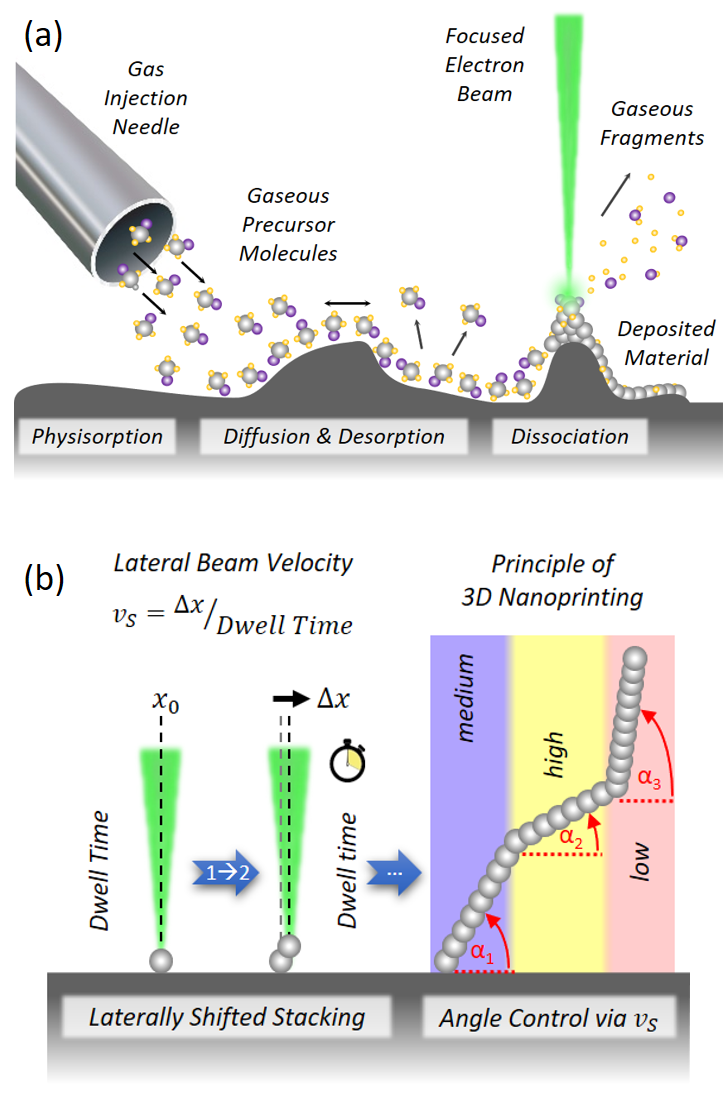
The aspiration of this CDL is to apply 3D‑FEBID for radically new application concepts concerning 3D nano-probes for advanced AFM operation. As conceptually shown in Figure 1.a, the technology relies on the highly localized dissociation of gaseous precursor molecules, which are physisorbed on the surface. Predictable 3D nano-printing becomes possible via the precise control of lateral beam movements, as briefly shown in Figure 1.b. Together with the increasing number of different precursor materials, this technology evolved into a nanofabrication tool-box with currently unrivaled 3D possibilities at that scale[2]. Of particular relevance for our industrial partners is the single-step fabrication of complex nanoprobes on pre-finished cantilevers, which can barely or even not at all be produced by alternative approaches. During the course of the CDL, we have developed different concepts, starting with electrical conductive nano-probes (Figure 2.a) for Conductive AFM (C-AFM). The differences to commercially available products are the coating free character due to the all-metal composition, together with sharp apexes in the sub-10 nm range[5]. As evident in Figure 2.b by a direct comparison, the performance of our nano-probes is much higher concerning lateral resolution but also in terms of durability. These nano-probes are meanwhile commercially available by our partners and leverages their AFM systems into the next level due to the unique selling point. Another application, which is currently close to commercialization are magnetic nano-tips (Figure 2.c) for Magnetic Force Microscopy (MFM). As for CAFM tips, the MFM nano-probes reveal all-metal character and sharp apexes in the same range, which enables a strongly improved magnetic sensitivity, as shown in Figure 2.d by a direct comparison to a commercial product. Due to 3D-FEBID’s strengths, more complex 3D nano-geometries become possible, which led to the introduction of an entirely new application concept for thermal probing. As shown in Figure 2.e, multi-leg structures with branch diameters of less than 100 nm are used as electrical nano-bridges, which changes the electric resistance with temperature. Due to the small volumes, thermal response is very fast (< 30 ms/K), which allows dynamic high-resolution studies[6].
Figure 2: 3D-FEBID based Nanoprobe Concepts. (a) tilted SEM image of an all-Platinum nano-probe with apex radii below 10 nm (see TEM inset top left), intended for C-AFM. (b) shows 500 nm wide morphology scans of an Au nanoparticle sample, performed with a commercially available standard C-AFM tip on top and the FEBID C-AFM tip at the bottom, where the massive resolution improvement becomes clearly evident. (c) shows a SEM side view of a magnetic nano-tip, again with apex radii in the sub-10 nm range. (d) shows 2.5 µm wide, magnetic phase-signals of a PtCo sample, acquired with a commercially available standard MFM tip (top) in direct comparison to the FEBID-based MFM tip, where the strong improvement is again clearly evident. (e) shows a SEM side view image of a FEBID-based 3D nano-bride together with a top view as inset. The electric current through the sub‑100 nm wide branches is temperature dependent and therefore informs about the surface temperature during AFM operation.
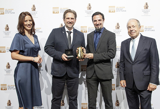
By that, 3D FEBID has fulfilled a long-lasting promise and finally found its way into commercial products due to currently unique possibilities, protected by broad generic patent[7]. That progress was also recognized by the B&C Holding, which awarded Harald Plank with the 1st price of the Houska Award 2020 in the area Academic Research, which is the most prestigious private award in Austria[8]. Fueled by the collective achievements, the CDL is now focusing on further concepts, which are currently not available on the market but planned to be introduced until the end of the CDL in 2025.
References
[1] GETec Microscopy GmbH & Quantum Design Microscopy, Darmstadt, Germany, AFSEM nano GETec | Quantum Design (qd-europe.com)
[2] “3D Nanoprinting via Focused Electron Beams”, R. Winkler, J.D. Fowlkes, P.D. Rack and H. Plank; Journal of Applied Physics 2019, 125 (21), 210901.
[3] Christian Doppler Gesellschaft, Vienna, Austria, Christian Doppler Forschungsgesellschaft: Christian Doppler Forschungsgesellschaft (cdg.ac.at)
[4] Anton Paar GmbH, Graz, Austria, Österreich :: Anton-Paar.com
[5] “3D Nanoprinting of All-Metal Nanoprobes for Electric AFM Modes”, L.M. Seewald, J. Sattelkow, M. Brugger-Hatzl, G. Kothleitner, H. Frerichs, C. Schwalb, S. Hummel and H. Plank; Nanomaterials 2022, 12 (24), 4477.
[6] “Three-dimensional nanothermistors for thermal probing”, J. Sattelkow, J.E. Fröch, R. Winkler, S. Hummel, C. Schwalb and H. Plank, ACS Applied Materials & Interfaces 2019, 11 (25), 22655.
[7] Patent “Multifunctional nanoprobes for scanning probe microscopy”, H. Plank, J. Sattelkow, R. Winkler, C. Schwalb; US Patent Nr. 11454648.
[8] Houskapreis – B&C Gruppe (bcgruppe.at)
Industrial Partner
Funding Agency & CDL Period
Thematic Cluster



GETec Microscopy GmbH
Am Heumarkt 13 | 1030 Vienna | AUSTRIA
Web: getec-afm.com
Email: info@getec-afm.com
Anton Paar GmbH (discontinued)
Anton-Paar-Straße 20 | 8054 Graz | AUSTRIA
Web: anton-paar.com
Email: office@anton-paar.com
Christian Doppler Gesellschaft
Boltzmanngasse 20/1/3, | 1090 Wien | AUSTRIA
Web: cdg.ac.at
Email: office@cdg.ac.at
Funding Period: 1.3.2018 – 28.2.2025
Advanced Materials Science
Development of new materials and processes
Microanalytics and nanoanalytics, structure determination
Materials modelling
