Materials scientists try to develop alloys and steels that are lighter, stronger and more durable during their use. Therefore, the knowledge of the microstructural characteristics such as crystalline phases, presence of secondary phases and elemental distributions is mandatory for new products. Electron microscopy is the ideal method to analyse metals and similar materials in a multi-scale approach ranging from the micrometre to the atomic scale.
Metals, Alloys & 3D Printed Materials
How can we help you?
• Defect Analysis / Fracture Analysis
• Microstructure Investigation
• Phase Identification by X-Ray Analysis
• Orientation Analysis of Crystal Grains
• Precipitate Analysis in Steels and Alloys
• Interface Analysis
• Defect Structures at Atomic Resolution
• In situ Heating Experiments (up to 1300°C)
• Structural and Chemical Mapping in 3D
Your Contact Details

Dr. Ilse Letofsky-Papst
Group Leader TEM
Tel. +43 316 873-8330
Contact me

Dr. Stefan Mitsche
Key-Account-Manager –
Metals, Alloys & 3D Printed Materials
Tel. +43 316 873-8831
Contact me
Fracture analysis
Materials produced in industry are all subject to fracture. Many of the failures are of special concern because of safety, environmental or legal considerations. Especially, the scanning electron microscope with X-ray spectrometry plays a central role in order to find the reason for failures. Additionally, we have established a fractography database which contains light microscopy, SEM, AFM, and TEM images in combination with mechanical data which helps us to identify materials failures fast and reliable.
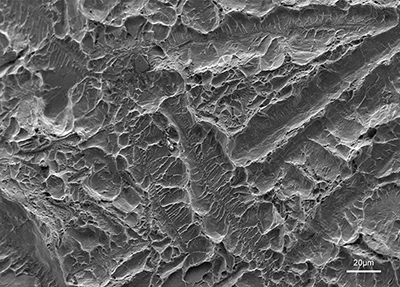
SE image of a rock candy fracture in steel casting with AlN precipitates
Phase identification by elemental mapping
The detailed characterisation of bond failures by means of electron microscopy and X-ray spectrometry (SEM-EDX) helps to improve bondability and reliability of wire bonds in microelectronics.
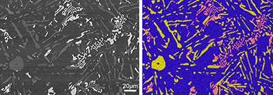
Elemental distribution map of precipitates in an Al-Si alloy, SE-image and X-ray elemental maps (blue = Al, yellow = Si, red = Fe)
Orientation analysis of crystal grains
Heat treatments leading to recrystallisation of steels and alloys are often used to tune the mechanical properties of these materials. Electron backscatter diffraction (EBSD) in the SEM allows the detailed investigation of the grain structure of superalloys, steels and light metals after homogenisation and hot forming. It also elucidates direct neighbourhood relationships between crystal grains.
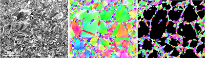
Recrystallisation of a Ni-base alloy investigation by SEM-EBSD; a. BSE-image, b. EBSD inverse pole figure map after deformation, c. inverse pole figure map of the recrystallized fraction.
Precipitate analysis in steels and alloys (1)
A very important problem in materials science is the visualisation of secondary phases embedded in a crystalline matrix e.g. precipitates and grain boundary phases in steels and alloys. The characterisation of their stereological parameters (size, distribution and volume fraction), chemistry and crystallography is best done in a TEM, which is additionally equipped with EDX- and EELS-spectrometers.
Energy-filtering TEM investigation of precipitates in a 9% chromium steel, TEM image with EFTEM elemental maps superimposed in an RGB image: red = V, green = Mn, blue = Cr.
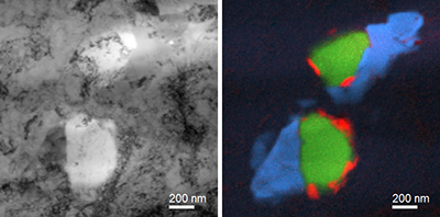
Defect structures at atomic resolution
Aberration correction opened a new frontier in electron microscopy analysis providing atomic resolution imaging and analysis. We operate the unique ASTEM (FEI Titan 60-300 kV), which is equipped with a Cs-probe corrector (FEI-Titan 60-300). In combination with improved specimen preparation and advanced data analysis and simulation methods, we are able to study structural details in alloys like twins, grain boundaries, defects and interfaces.
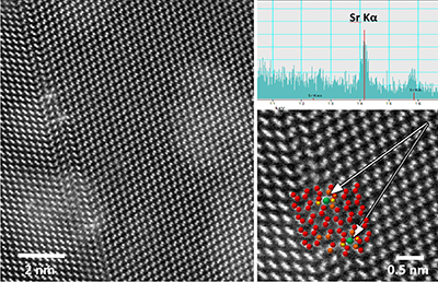
Silicon eutectic phase in Al-Si alloy doped with Sr, STEM-HAADF-images reveal Sr on interstitial positions within the twins (with EDX spectrum and structure model)
Precipitate analysis in steels and alloys (2)
Electron diffraction allows to study the crystal structure of secondary phases in materials. Compared to X-ray diffration, it has the advantage of high spacial resolution down to the nanometre regime.
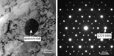
TEM image of an individual quasicrystalline precipitate in a melt spun Al-alloy, electron diffraction pattern taken along the fivefold axis of the precipitate (Christian Gspan)