Ceramic systems are processed by sintering different oxides and other mineral substances into finely structured building blocks. The properties of the final components and articles are influenced by grain sizes, microstructures and textures. New developments as well as unexpected defects can be detected efficiently by means of SEM as well as modern microscopic-spectroscopic correlated methods (e.g. our RISE system). In addition, you can also observe and design the sintering process with us in in situ heating investigations.
Ceramic Systems
How can we help you?
• Error Analysis
• Quality Control
• Phase Analysis by Means of X-Ray and Raman Spectroscopy
• Microstructure Characterization
• Grain Size Determination
• Texture Analysis
• Grain Boundary Interface Analysis
• Defect Analysis down to the Atomic Level
• In situ Heating Investigations
Your Contact Details

DI Dr. Stefan Mitsche
Key-Account-Manager – Ceramic
Tel. +43 316 873-8346
Contact me

Ing. Hartmuth Schröttner
Gruppenleiter REM/IR/Raman
Tel. +43 316 873-8349
Contact me
Crystal Orientation Analysis
By means of electron backscatter diffraction (EBSD) using a scanning electron microscope (SEM) it is possible to perform grain size determinations, texture and grain boundary analyses of crystalline materials.
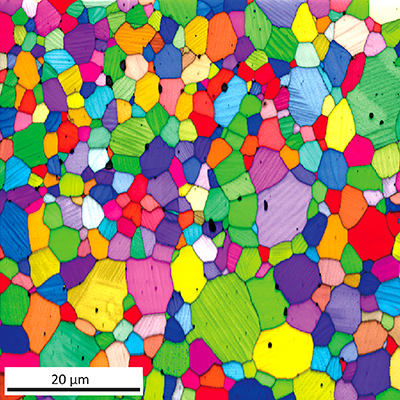
SEM-EBSD of a Nickel Praseodymium Oxide Ceramic: Colour Coded Crystal Orientation
Phase Analysis
In addition to elemental analysis, it is possible to perform a direct phase determination/distribution using different techniques at FELMI-ZFE.
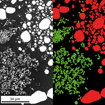
SEM-Raman Phase Analysis by Means of Machine Learning, Red: WO3, Green: WS2
Defect Analysis
Defects such as cracks, pores, impurities but also grain boundary dislocations can be analyzed from the mm- to the µm- down to the atomic range using light microscopy (LiMi), scanning electron microscope (SEM) and transmission electron microscopy (TEM).
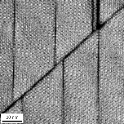
HRSTEM-HAADF: Crystal Dislocation in Lanthanum Barium Ferrate
Crystal orientation analysis
By means of electron backscatter diffraction (EBSD) using a scanning electron microscope (SEM) it is possible to perform grain size determinations, texture and grain boundary analyses of crystalline materials.
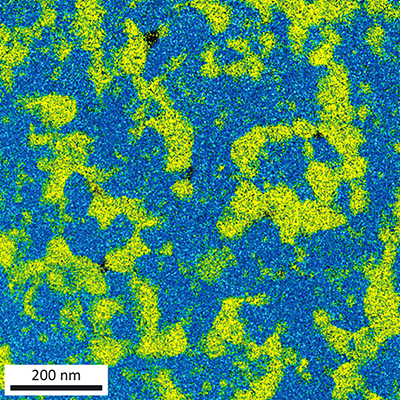
STEM-EDX Elemental Mapping of BaCe0.4Fe0.4Y0.2O3
Blue: Fe, Yellow: Ce