ZFE is one of the leading materials characterisation experts for the semiconductor industry. Relying on a profound experience in device and failure analysis in microelectronics, we focus on new characterisation methods mostly based on electron microscopy (SEM-EDX-WDX-EBSD, FIB-processing and STEM-EDX-EELS-EFTEM). We continuously provide services for leading semiconductor companies and co-operate with them via national and European research projects.
Electronics and Semiconductors
How can we help you?
• Defect Analysis, Quality Control
• Multi Layer Systems and Interfaces
• Materials Characterisation
• HRTEM Analysis (Structure Defects)
• In situ Experiments, (Heating Experiments, Ageing)
• Device Modification
• 3D Reconstructions
• Site Specific Cross Section Analysis
Your Contact Details

DI Dr. Evelin Fisslthaler
Key-Account-Managerin –
Halbleiter
Tel. +43 316 873-8834
Contact me

Prof. DI Dr. Werner Grogger
Gruppenleiter TEM
Tel. +43 316 873-8323
Contact me
Reducing bond failures in
microelectronics
The detailed characterisation of bond failures by means of electron microscopy and X-ray spectrometry (SEM-EDX) helps to improve bondability and reliability of wire bonds in microelectronics. SEM evaluation and FIB cross-sectioning are also used to study the influence of high temperature or chemical effects on bond wires.
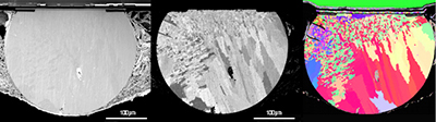
Wire bond investigated by scanning electron microscopy, secondary electron image, channeling contrast image (BSE) and backscatter diffraction (EBSD) image.
Site specific metrology in semiconductor analysis
Development and testing of semiconductor devices requires extensive knowledge of local structures with high accuracy. Typically, cross-sections of the devices are site-specifically prepared with the focused ion beam technology (FIB milling) and the TEM characterisation involves classical TEM techniques and advanced atomic resolution STEM.
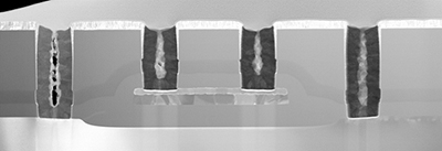
STEM-HAADF image of a large area cross-section of a semiconductor device.
Nanoanalysis of semiconductor devices
Information about the elemental composition is critical for identifying anomalies that cause the semiconductor devices to fail. Here, the STEM in combination with EELS and EDX is one of the most powerful methods. EELS and EDX spectrum imaging help to better understand materials complexities and failures to improve device performance.
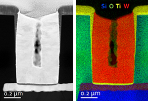
STEM-HAADF investigation of a tungsten plug in an integrated circuit; with electron distribution map (RGB-image) derived from an EDX-spectrum image revealing the elements Si, O, Ti and W.
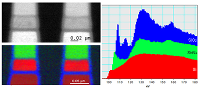
STEM-EELS analysis of the chemical phases in a semiconductor device (blue = SiO2, green = Si3N4, red = Si); HAADF-image with chemical phase map by MLLS fitting of a Si L edge spectrum image using the ELNES-changes and core level shifts.