The NOVA 200 Nanolab is a FIB / SEM dual beam microscope with various possibilities in structural and chemical high resolution imaging (secondary electrons: SE, backscattered electrons: BSE, X-rays), in-depth analyses & 3D reconstruction, 3D structuring down to the nanoscale and ultrathin TEM lamella preparation.
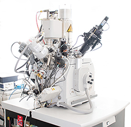
FIB/SEM Dual Beam Microscope FEI NOVA200
Key Features
- Dual beam conception for direct observation of ion beam related processes such as milling / deposition / etching
- High resolution scanning electron beam microscope
- Site specific TEM lamella preparation (< 50 nm thickness)
- Fabrication of conductive (Pt) and insulating (SiOx) nanostructures (< 20 nm) via particle induced deposition from the gas phase
- Negative nanostructuring via direct milling or particle assisted etching (via etch gases)
- Chemical and structural 3D reconstruction via automated slice & view procedures
- Low temperature processing via cryo stage
- Device modification
Essential Specifications
Resolution
• 1.5 nm@ 15 keV (eucentic WD)
• 2.5 nm@ 5 keV eucentric WD)
• 2.5 nm@ 1 keV (optimum WD)
• Ions: 7 nm@ 30 kV (eucentric)
Emitter
• Electrons: Thermal Field Emmision Gun (FEG)
• Ions: Ga liquid metal source
Accelerating Voltage
• Electrons: 1 – 30 kV
• Ions: 5 – 30 kV
Probe Current
• Electrons: 2.5 pA – 37 nA
• Ions: 1 pA – 20 nA
Detectors
• In-lens SE / BSE Detector
• Everhart Thornley SE / BSE Detector
• EDS Detector Bruker
Ions
• In-lens SE / BSE Detector
• Everhart Thornley SE / BSE Detector
• Direct Ion Detector
5-Axes Motorised Eucentric Specimen Stage
• X=50 mm/Y=50 mm/Z=25 mm
• Tilt = -15 – 60
• Rotation = 360° (continuous)
Dual Beam Features
• Direct ion beam milling:
⇒ Minimum line width: <25 nm on Au
⇒ Maximum aspect ratio: ~ 10:1 (on Si)
• Automated slice and view for sequential milling and SE / BSE imaging or X-ray mapping for 3D reconstruction
• Particle included deposition of conductive Pt, Au or insulating SiOx from the gas phase with minimum line widths:
⇒ <20 nm for electron beam induced processes
⇒ <50 nm for ion beam induced processes
• Particle assisted etching via I2 and XeF2 gases (preferably for conductive and insulating materials respectively):
⇒ Minimum line width: < 15 nm (on Si)
⇒ Maximum aspect ratio: ~ 20:1 (on Si)
• Special flange for custom gas injection (particle assisted processes, purification purposes during deposition, sensor applications, …)
• 16-bit patterning engine working with:
⇒ Implemented patterning tools
⇒ Bitmaps
⇒ Direct beam control (stream files)
• Temporal resolved current measurement via sample stage (down to pA range)
• Cryo temperature sample holder
• 4-axes micromanipulator (OmniprobeTM)