A Review on Direct-Write Nanoprinting of Functional 3D Structures with Focused Electron Beams
Volume 34, Issue 46, November 12, 2024 Cite this article
Abstract
Following Moore`s law, the performance of devices should double within a two-year span, which can either be done by reducing the size of the individual components or adapting the working mechanism. In most cases the same mantra applies – pushing the size while keeping the quality. As manufacturing techniques are approaching the atomic scale, however, miniaturization reaches its intrinsic limit, shifting focus toward higher-dimensional architectures realized by stacking planar layers or fabricating true, free-standing nanostructures. A mask-less, additive manufacturing technique with the capability to produce such 3D structures at the nanoscale is called Focused Electron Beam Induced Deposition (FEBID). Applying a focused electron beam in a conventional scanning electron microscope together with a gaseous metal-precursor gives access to a vast library of complex, 3D nanostructures, which exhibit feature sizes down to the 10 nm-range and can be printed in a single step on most substrates. This review aims at introducing the technique to a broader scientific community, breaking down the most important processing routes and highlighting disciplines explored so far ranging from nanooptics and nanomagnetism, over scanning probes and field emitters to sensing and particle trapping. Finally, a future roadmap of the technique is discussed, and prospective research focus identified.
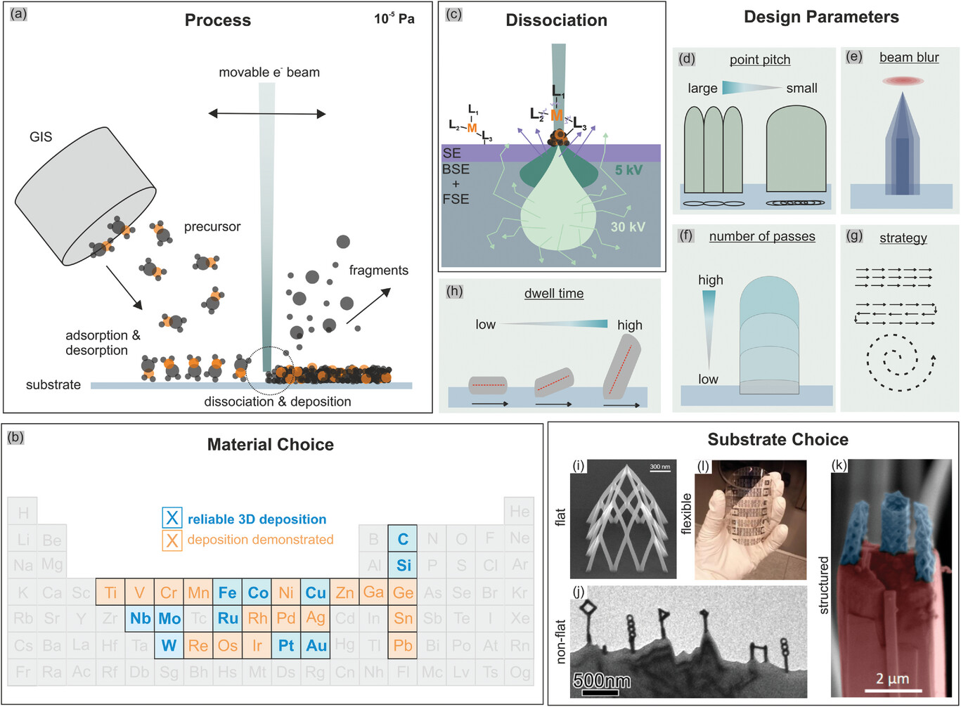
Figure 1. FEBID principle. a) Heated precursor gas is continuously introduced via a gas injection system (GIS) in close proximity to the working surface,
where it physisorbs and covers the targeted area. Once equilibrium adsorption is reached, the electron beam is focused onto a specific spot, initiating
local dissociation of the irradiated precursor. These molecules split into a volatile part which is being pumped out by the vacuum system, and a solid
part, which, step by step forms the intended structure. b) Overview of the periodic system where only for colored elements suitable FEBID precursors
exist. For the ones colored in orange FEBID deposition has in principle been demonstrated.[30,32,34,35] The ones colored in blue can be readily applied
for the fabrication of 3D structures (iron,[36] cobalt,[37] copper,[38] carbon,[39] silicon,[40] niobium,[41] ruthenium,[42] tungsten,[43] platinum,[44] gold[45]).
c) Interaction volume exemplarily shown for low (5 keV) and high (30 keV) acceleration voltages and its implications concerning beam diameter and
electron range. Important design parameters for the fabrication of FEBID nanostructures being d) point pitch, e) beam blur, f) number of passes,
g) patterning strategy and h) dwell time. As a consequence of the mask-less approach, FEBID can be performed on various different morphologies
of substrates including i) flat, j) non-flat, k) structured, and l) flexible ones. a) adapted with permission.[46] Copyright 2024, The Authors. Advanced
Functional Materials published by Wiley-VCH GmbH; i) reproduced with permission.[17] Copyright 2019, AIP Publishing; j) adapted with permission.[47]
Copyright 2005, IOP Publishing; k) adapted with permission.[45] Copyright 2016, American Chemical Society; l) adapted with permission.[48] Copyright
2015, American Chemical Society, https://pubs.acs.org/doi/full/10.1021/acsnano.5b01383, further permissions related to the material excerpted should
be directed to the ACS.